OEM Solutions
OEM SOLUTIONS
OEM Solution
Streamlining processes are one of the most important aspects in ensuring increased productivity in this challenging industry. Our OEM total solution provides you all you need in establishing a full-scale, fully automated production. We leverage our diverse technical and engineering knowledge to build the right automation solutions for you.
- Raw material: sourcing & supply
- Electrical & electronic
- Mechanical review
- Module assembly
- Test & debugging
- Service & support
OEM Total Solution


More Our Solutions
OEM Total Solution
Talk to us for more details about our solutions.
Automation solution
Automation solution
Automation solution
As the manufacturing industry becomes more challenging and demands more output, automation is now essential. We have the ability and skills to create automated turnkey factory solutions. We build end-to-end systems that can be easily implemented onto production floors.

More Our Solutions
Talk to us for more details about our solutions.
Blauwal
Blauwal
Blauwal
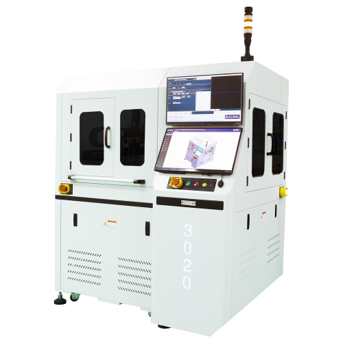
In order to optimize manufacturing processes, vision inspection is an essential process to ensure extremely high accuracy. We’re able to assemble vision inspection machines to your satisfaction, equipped with the right vision software for the job. Blauwal’s vision software is our trusted software to enhance efficiency.
- Wafer inspection
- Micro/Mini LED inspection
- Skeleton Wafer inspection
- 3D Line scan
- IR/SWIR inspection

More Our Solutions
Talk to us for more details about our solutions.
Wafer Solution
WAFER SOLUTION
Wafer solution
Throughout the years, we have been working with wafers to produce the best wafer solution. Wafer, also known as a slice or substrate is a thin slice of semiconductor used in integrated circuits. These wafers work as substrates for microelectronics components to be built in and on the wafer.


Wafer sorting
Wafer sort is a testing procedure performed on a silicon die in a wafer form. This is to identify non-functional dies. Over the past decade, wafer testing has evolved to include the use of automation equipment and test technologies. We had an abundance of experience in wafer sorting/testing and are confident to help you find the right solutions to speed up productivity.

Wafer inspection
Wafer inspection is a system for detecting physical defects (foreign particles) and pattern defects on wafers. Using the Blauwal vision system solution, wafer inspection can be done by comparing the image of patterns and dies. In a nutshell, the wafer inspection detects imperfections on a wafer and finds out their position coordinates.

Wafer marking
Wafer markings are used to imprint wafers to allow tracking wafers through the processes of manufacturing. The wafer marking requires high accuracy, fast speed, and permanent marking qualities. By using laser marker technology, the markings ensure high cleanliness for traceability and reliability of the wafers.
More Our Solutions
Talk to us for more details about our solutions.
Metal & Fabrication
Metal & Fabrication
Metal & Fabrication
The smallest component plays a huge part in your daily operations in this aggressive industrial market. With great lead time and years of experience, TTOT promises ultra-high precision in every component we provide.
- CNC
- Milling
- Grinding
- EDM
- Wire cut


